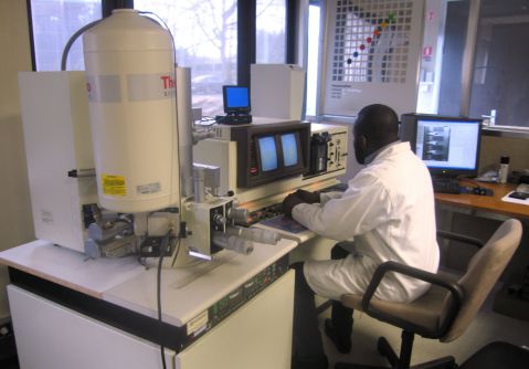
SEM enables very high magnification observations (>100000) of materials and electrically conductive components. Non electrically conductive or insulators shall be Au-Pd or carbon plated to be analyzed.
The EDS probe provides a qualitative indication of the different elements constitutive of a sample as well as a semi-quantitative analysis, from the βe. Thanks to the X mapping functionality, it also enables to obtain a visual distribution of these elements within the analyzed sample.
SEM and EDS ANALYSIS:
To better meet our customer needs and face the increasing trends towards electronic component miniaturization, the CERB company invested in a Scanning Electron Microscope (SEM) from HITACHI coupled to an EDS probe.


Choisissez votre langue
Choose your language


SEARCH ON THE WEBSITE
Copyright 2013